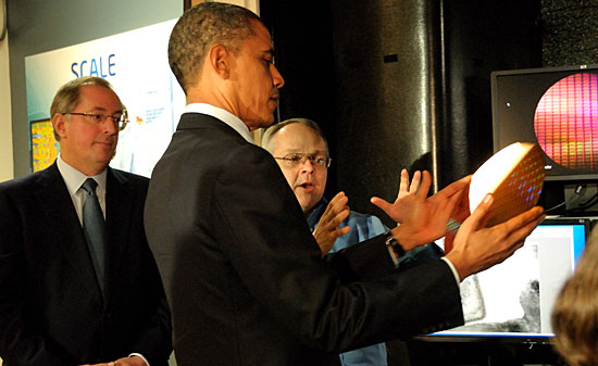
 Future At Intel - three strong words, summarized into one word = Awesome! Intel hosting one of the world's most powerful man on Earth is just uber pimp. President Obama visited Intel to emphasize how technology and innovation can make for better future. President Obama met with CEO Paul Otelinni who announced that Intel will build a new Fab at Arizona. This means more employment, not to mention more Fab means better output for Intel and better output means more mass-produced processors and that could lead to even more cheaper and more innovative products! Check out the video at the White House Blog below...
Showing posts with label technology. Show all posts
Showing posts with label technology. Show all posts
Monday, February 21, 2011
Tech Link (Industry): Weekly Address: Winning the Future at Intel
Future At Intel - three strong words, summarized into one word = Awesome! Intel hosting one of the world's most powerful man on Earth is just uber pimp. President Obama visited Intel to emphasize how technology and innovation can make for better future. President Obama met with CEO Paul Otelinni who announced that Intel will build a new Fab at Arizona. This means more employment, not to mention more Fab means better output for Intel and better output means more mass-produced processors and that could lead to even more cheaper and more innovative products! Check out the video at the White House Blog below...


Wednesday, June 13, 2007
Tech Link (Processor): Clovertown versus Barcelona
 RickGeek of Geek.Com posted an interesting opinion about native versus mcm. In his post, the author cited many advantaged/disavantages of Clovertown MCM versus the competition's so called offering. And the truth isn't very hard to see, Intel has been shipping millions of quad core processors while AMD has yet to ship one. And I don't mean sample, Intel is shipping retail products, just in case you're not aware yet, and AMD is still delaying their Barcelona release. This processor better perform or it will be a major dissapointment even for a FanBoy like me...
OPINION
When I first heard about AMD's decision to make a native quad-core processor--that is a single piece of silicon comprising all four cores--I thought it was an excellent idea. I began to think of the advantages four-way HyperTransport has over the shared bus architecture of Intel's design. I also saw the significance in the larger shared cache, especially when all four cores are working closely on some particular task, and I didn't really see any downside. However, the more I think about it, the more I am realizing how much better Intel's solution is.
Clovertown is a single-package solution comprising two dual-core Core 2 processors within. It uses a shared bus architecture and is somewhat slower in off-chip communication, but because the die is so much smaller, they can create a larger shared cache for each dual-core, thereby making up for much of that loss.
AMD is not at the same place in manufacturing prowess that Intel is. It has been reported that Intel's yields are also very high, typically 90% or higher with some reports saying 95% or higher. AMD's yields have never (to my knowledge) been publicly disclosed, though I'm going to make a probably very incorrect assumption that they're around 80% for current processors. Even assuming they were 95% for current processors, we know that the number of potential defects goes up by the square of the surface area, so as we move from K8's current 183 mm^2 dual-core 65 nm 512 KB L2 processors, we would see a significant degredation in potential yield due to an additional 100 mm^2 per die alone. That also does not include the potential loss of high-binning parts due to even small defects not making the chip unusable, but rather making them less clockable at higher speeds.
We now know that Barcelona's die will be 283 mm^2, and that Clovertowns are comprised of two 143 mm^2 dual-core dies. Using my Wafer program, we find that AMD could fit a maximum of about 212 Barcelonas per 300 mm wafer, while Intel could fit about 430 dual-core Core 2 processors on a single 300 mm wafer. Now, assuming a 90% yield for Intel, that's about 388 dies per wafer, or 194 Clovertowns. In order for AMD to make as many Barcelonas per 300 mm wafer, its yield would have to be 92%, and by all accounts that's not something AMD will be able to do 1) based on its unconfirmed history of lower yields, 2) based on the natural increase in defect rate due to the larger die size and 3) that defects of any kind which do not render the chip inoperable will render it operable only at slower speeds.
AMD is facing several realities here with its native quad-core design, and it would seem that it does not have the manufacturing prowess to pull it off. Some at Intel even admitted recently that the company would have a hard time doing a die that large with high yields. Note also that Intel's Itanium at its largest on an 180 nm process technology was about 473 mm^2, quite a bit larger. I believe that also might explain why Intel targeted the highest-end markets with Itanium--because those processors sold for so much that very low yields would still be profitable.
As we stand today, with a pricing war going on between Intel and AMD, this native quad-core does not seem to provide enough financial incentive for AMD to have gone with it, even with its potentially much higher performance and scalability.
I see no two ways about it; I think AMD has made a significant mistake in going with the native quad-core design. Had it gone with an approach similar to Intel's, the company could've already had single-package quad-core parts out the door, and their yields would've been greater, their processing power would've only been slightly slower, and they could've been more price competitive.
As it stands, I just don't see the advantages of a native quad-core design. However, I'd very much like to hear your opinions.
Please post your thoughts below.
Source:Clovertown versus Barcelona
Monday, June 11, 2007
Tech Link (Technology): Intel discusses quad-core processor server market
 An interview with Intel GM for Server Platforms Group is posted by Digitimes and in that interview, the GM mentioned his thoughts about the competition's native quad core future offering. Expand to read the Q&A...
Shawn Chen, Taipei; Joseph Tsai, DIGITIMES [Friday 8 June 2007]
With AMD and Intel pushing their quad-core server processors at Computex Taipei 2007, Digitimes got a chance to talk to Boyd Davis, general manager of server platform group marketing of Intel to discuss Intel's plans and thoughts about the new quad-core processors.
Q: What was the main factor that caused Intel to bring its 45nm Harpertown server processor forward to this year?
A: Intel's product launch is directed by the demand of clients, which has nothing to do with the competition in the market. Currently, product development is almost complete therefore it is natural for the company to launch the Harpertown processor ahead of schedule. The company expects to mass produce the processor in the fourth quarter this year.
Q: In the current server market, competition among CPU makers over semiconductor technology has boosted the migration rate of new platforms. Can the enterprise market catch up in technology?
A: In the past, the server product lineup had a slow migration rate due to the long research time in developing the processor. However, with the assistance of nanometer processing, CPU technology now can advance faster, which shortens the product manufacturing time, sequentially. Intel used to have CPU as the unit for server migration in the past, but is now using platforms. The current platform is expected to last until Penryn processor launches in the fourth quarter.
Q: What are Intel's thoughts about the delay of AMD's native quad-core processor Barcelona?
A: AMD's so-called native quad-core processor has a difficult challenge in technical and manufacturing terms and even Intel would have difficulty facing such challenges. Intel currently still adopts two dies on one chip for its Harpertown processor. The technology is much easier, the product has higher yields and performance is almost the same as the native quad-core processor. Therefore, Intel will continue to use this design in 2007.
Q: With the server market currently crossing over several different fields, besides the enterprise sector, in what markets do you expect to see good performance?
A: Other than the enterprise market, HPC (high-performance computer), blade server and workstation sectors are all expected to have good performance. In the past, middle and small enterprises had the highest server adoption rates, but now demand for HPCs, blade servers and workstations is increasing due to demand from multimedia and Internet search engines and the Internet communication markets. These fields are expected to perform better than others.
Source:Intel discusses quad-core processor server market
Wednesday, May 30, 2007
Tech Link (Event): XtremeSystems @ Computex
 Looks like there will be lots of overclocking session in the upcoming Computex 2007 event. I am looking forward to seeing new innovative products from different vendors, from the typical to the extra ordinary. Anyway, I am getting a bit carried away, XS team is invited and will be at the site for some live demonstration power of overclocking. Check out the thread at XS.
Friday, April 20, 2007
Tech Link (Industry): AMD: Blood In The Streets, Gross Margin At 31%
 I have nothing to add, I'll just let AMD*'s CFO deliver the message, expand to read the WallSt source article.
“After more than three years of successfully executing our customer expansion strategy and significantly growing our unit and revenue base, our first quarter performance is disappointing and unacceptable,” said Robert J. Rivet, AMD’s chief financial officer-source
AMD: Blood In The Streets, Gross Margin At 31%
AMD (AMD) rallied like a house afire, closing the regular session at $14.28. up 2.7% on over 50 million shares, about double its normal volume.
AMD reported revenue of $1.233 billion and a GAAP loss of $504 million. In the quarter a year ago, revenue was $1.33 billion and the company had a profit of $259 million.
Gross margins fell to an unbelieveable 31%. In the same quarter a year ago, they were 59%. In Q4 06, 40%.
The company expects the next quarter to be flat.
The company's cash dropped to $1.167 billion from $1.541 billion at the end of last year. Receiveables dropped from $1.14 billion to $667 million. Never a good sign.
Advanced Micro Devices was expected to report a loss of 48 cents per share for the first quarter. Analysts on average, expect AMD to report a 5 percent sales decline to $1.26 billion
The company this month forecast sales of $1.22 billion after last month saying it was unlikely to meet its previous target for sales of $1.6 billion to $1.7 billion.
Douglas A. McIntyre
Source:AMD: Blood In The Streets, Gross Margin At 31%
Thursday, March 29, 2007
Press Release: Intel Details Upcoming New Processor Generations
 Chipzilla finally unleashes the official statement about its upcoming processor (Penryn) and upcoming microarchitecture (Nehalem). I'll post more on this later on, right now, check out the official Press Release (I'll format it later on)...
Intel Details Upcoming New Processor Generations
Marking the next step in Intel's "tick-tock" product strategy and cadence to deliver a new process technology with an enhanced microarchitecture or entirely new microarchitecture every year, Intel Corporation will begin producing its next-generation Penryn family of processors in the second half of this year. These new processors benefit from enhancements to the Intel® Core™ microarchitecture and also Intel's industry-leading 45nm Hi-k process technology with its hafnium-based high-K + metal gate transistor design, which results in higher performance and more energy-efficient processors.
Intel has more than 15 45nm Hi-k product designs in various stages of development, and will have two 45nm manufacturing fabs in production by the end of the year, with a total of four in production by the second half of 2008 that will deliver tens of millions of these processors. Below are many of the details of the Penryn processor family and a glimpse into some of the key features of Intel's future generation of processors, codenamed Nehalem.
PENRYN FAMILY MICROARCHITECTURE INNOVATIONS
- A Range of Products -- Six Penryn family processors, including dual and quad-core desktop processors and a dual core mobile processor are all under the Intel Core processor brand name as well as new dual and quad-core server processors under the Intel® Xeon® processor brand name. A processor for higher-end server multiprocessing systems is also under development. As previously noted, Intel already has a total of 15 45nm products scheduled.
- Technical Marvel -- 45nm next-generation Intel® Core™2 quad-core processors will have 820 million transistors. Thanks to our high-k metal transistor invention, think of 820 million more power efficient light bulbs going on and off at light-speeds. The dual-core version has a die size of 107mm2, which is 25 percent smaller than Intel's current 65nm products - and quarter of the size of the average U.S. postage stamp - and operate at the same or lower power than Intel's current dual core processors.
- Deep Power Down for Energy Savings, Improved Battery Life -- The mobile Penryn processor has a new advanced power management state called Deep Power Down Technology that significantly reduces the power of the processor during idle periods such that internal transistor power leakage is no longer a factor. This helps extend battery life in laptops. This is a major advancement over previous generation industry leading Intel mobile processors.
- Intel Dynamic Acceleration Technology Enhanced Performance for Single Threaded Apps -- For the mobile Penryn processor, Intel has enhanced the Intel® Dynamic Acceleration Technology available in current Intel Core 2 processors. This feature uses the power headroom freed up when a core is made inactive to boost the performance of another still active core. Imagine a shower with two powerful water shower heads, when one shower head is turned off, the other has increased water pressure (performance).
- Speeding Up Video, Photo Imaging, and High Performance Software -- Penryn includes Intel® Streaming SIMD Extensions 4 (SSE4) instructions, the largest unique instruction set addition since the original SSE Instruction Set Architecture (ISA). This extends the Intel® 64 instruction set architecture to expand the performance and capabilities of the Intel® Architecture.
- Other Technical Features to Improve Performance
- Microarchitecture Optimizations -- Increases the overall performance and energy efficiency of the already leading Intel Core microarchitecture to deliver more instruction executions per clock cycle, which results in more performance and quicker PC responsiveness.
- Enhanced Intel® Virtualization Technology -- Penryn speeds up virtual machine transition (entry/exit) times by an average of 25 to 75 percent. This is all done through microarchitecture improvements and requires no virtual machine software changes. Virtualization partitions or compartmentalizes a single computer so that it can run separate operating systems and software, which can better leverage multicore processing power, increase efficiency and cut costs by letting a single machine act as many virtual "mini" computers.
- Higher Frequencies -- Penryn family of products will deliver higher overall clock frequencies within existing power and thermal envelopes to further increase performance. Desktop and server products will introduce speeds at greater than 3GHz.
- Fast Division of Numbers – Penryn-based processors provide fast divider performance, roughly doubling the divider speed over previous generations for computations used in nearly all applications through the inclusion of a new, faster divide technique called Radix 16. The ability to divide instructions and commands faster increases a computer's performance.
- Larger Caches -- Penryn processors include up to a 50 percent larger L2 cache with a higher degree of associativity to further improve the hit rate and maximize its utilization. Dual-core Penryn processors will feature up to a 6MB L2 cache and quad-core processors up to a 12MB L2 cache. Cache is a memory reservoir where frequently accessed data can be stored for more rapid access. Larger and faster cache sizes speed a computer's performance and response time.
- Unique Super Shuffle Engine -- By implementing a full-width, single-pass shuffle unit that is 128-bits wide, Penryn processors can perform full-width shuffles in a single cycle. This significantly improves performance for SSE2, SSE3 and SSE4 instructions that have shuffle-like operations such as pack, unpack and wider packed shifts. This feature will increase performance for content creation, imaging, video and high-performance computing.
NEHALEM MICROARCHITECTURE
After Penryn and the 45nm Hi-k silicon technology introduction comes Intel's next-generation microarchitecture (Nehalem) slated for initial production in 2008. By continuing to innovate at this rapid cadence, Intel will deliver enormous performance and energy efficiency gains in years to come, adding more performance features and capabilities for new and improved applications. Here are some new initial disclosures around our Nehalem microarchitecture:
- Dynamically scalable for leadership performance on demand with energy efficiency
- Dynamically managed cores, threads, cache, interfaces and power
- Leverages leading 4 instruction issue Intel® Core microarchitecture technology
- Simultaneous multi-threading (similar to Intel® Hyper-threading technology) returns to enhance performance and energy efficiency
- Innovative new Intel® SSE4 and ATA instruction set architecture additions
- Superior multi-level shared cache leverages Intel® Smart Cache technology
- Leadership system and memory bandwidth
- Performance enhanced dynamic power management
- Design scalable for optimal price/performance/energy efficiency in each market segment
- New system architecture for next-generation Intel processors and platforms
- Scalable performance: 1 to 16+ threads, 1 to 8+ cores, scalable cache sizes
- Scalable and configurable system interconnects and integrated memory controllers
- High performance integrated graphics engine for client
Click here to download this fact sheet as in PDF format. [PDF, 48KB]
Click here to listen to an audio interview with Pat Gelsinger, senior vice president and co-general manager of Intel Corporation's Digital Enterprise Group.
Intel, the world leader in silicon innovation, develops technologies, products and initiatives to continually advance how people work and live. Additional information about Intel is available at www.intel.com/pressroom.
Source:Intel Details Upcoming New Processor Generations
Saturday, March 24, 2007
Tech Link (Industry): Intel vs. AMD: Today's generation compared
 Want to feed your FanBoyism even more? Then check out the latest article from TheTechReport. I enjoyed reading the Conclusion part, so I never bothered reading the rest of the article. Well, they are a pretty good site, more trustworthy than AMDTech, so check out their great article and indulge yourselves.
Conclusions
The fact that Intel retains the overall performance crown comes as no surprise. As we said at the outset, AMD has no real answer to the Core 2 Extreme X6800 among its dual-core processors. Also, Intel's quad-core CPUs tend to scale better than AMD's Quad FX platform, especially for typical desktop-class applications. Our move to Windows Vista x64 has done little to alter this dynamic. At the same time, Core 2 processors tend to draw less power and to be more energy efficient—sometimes markedly so—than Athlon 64s. Right now, Intel has the magic combination of a superior processor microarchitecture and a more mature, fully realized 65nm manufacturing capability working together on its side.
This one-two punch has allowed Intel to maintain a performance edge at most price points, despite standing pat through AMD's aggressive pricing moves and new model introductions. AMD's current weaknesses manifest themselves most fully in its high-end models, like the Athlon 64 X2 6000+, which draws more power at peak than the Core 2 Extreme QX6700 yet is often outperformed by the less expensive Core 2 Duo E6600. The Athlon 64 looks more competitive in its lower-end incarnations like the X2 5000+ and 4400+, which match up better on both performance and power characteristics against the Core 2 Duo E6300 and E6400. These processors have the benefit of being available in 65nm form, and I'd say the minor performance penalty one pays in performance at 65nm (due to the slower L2 cache) is worth it for the reduced power draw.
This low-to-mid-range territory, incidentally, is where I'd be looking to buy. Many of our tests have shown the benefits of quad-core processors, but honestly, finding applications that will make good use of four cores is not easy—and the list of games that really use four cores is approximately zero. I'd probably grab a Core 2 Duo E6400 and overclock it until it started to glow, if I were putting together a system right now. I must admit, though, that I have an almost irrational fondness for the Core 2 Quad Q6600, probably because it's the most energy efficient processor in our Cinebench power test. The thing is by no means a great deal—two E6600s will set you back over $200 less than a single Q6600—but it's easy to imagine a near-silent multitasking monster built around one.
AMD would do well to expand its 65nm offerings into higher clock frequencies as soon as it can reasonably do so. That may take a while yet, given the limited overclocking headroom we've seen from early 65nm Athlon 64 X2s. Meanwhile, Intel isn't likely to sit still for much longer. Rumors of an April price cut abound, and in light of the Core 2's ample frequency headroom, higher speed grades are a definite possibility, as well. For AMD, its next-generation microarchitecture can't come a moment too soon.
Source:Intel vs. AMD: Today's generation compared
Questions asked, questions answered
Thursday, February 15, 2007
Tech Link (Technology): Intel Says 45 Nanometer Microprocessors Due Later This Year
 I just stumbled upon this link after a friend directed me to it. It's a very nice video, providing a lot of information about the 45nm technology from Intel. I have embedded it here in my Blog, but I also provided the true source of this link. I really love the "documentary"-style video, and I hope more will be made in the future. Enjoy (and ensure you have good broadband).
Intel announced that it will begin making 45 nanometer chips, code-named Penryn, in the second half of the year. The new microprocessors are the culmination of years of R&D using new materials to improve the efficiency and performance of silicon-based semiconductors.
The company says the new chip technology maintains Moore's Law, the observation made by Intel co-founder Gordon Moore in the late 1960s that the number of transistors doubles on chips every two years. Intel scientists say that transistors are now so small that more than 300 can fit on a human red blood cell.
In a recent earnings announcement, Intel officials said they expect to rebuild a lead in the computer chip market through innovation and manufacturing efficiency. Intel's current line of microprocessors includes the Core2Duo, Core2Extreme, and Core2Quad.
In this video podcast, PodTech's Jason Lopez visits Intel's Hillsboro, Oregon research facility and fab.
Related Stories: IntelMooresLaw
Source:Intel Says 45 Nanometer Microprocessors Due Later This Year
Monday, February 12, 2007
Press Release: Intel Research Chip Advances 'Era Of Tera'
 This is so exciting, Intel just released another wonderful research to the wild and "wow" the world yet again. It feels good to finally discuss this in the open, well, at least the early information posted on the official website.
Imagine such powerful computing power, so massive, so advance, so futuristic. Welcome "Polaris", I am wating with anticipation. Expand to read the official Press Release.
Intel Research Chip Advances 'Era Of Tera'
80-Core Programmable Processor First to Deliver Teraflop Performance with Remarkable Energy-Efficiency
SANTA CLARA, Calif., Feb. 11, 2007 - Intel Corporation researchers have developed the world's first programmable processor that delivers supercomputer-like performance from a single, 80-core chip not much larger than the size of a finger nail while using less electricity than most of today's home appliances. This is the result of the company's innovative 'Tera-scale computing' research aimed at delivering Teraflop -- or trillions of calculations per second --performance for future PCs and servers. Technical details of the Teraflop research chip will be presented at the annual Integrated Solid State Circuits Conference (ISSCC) this week in San Francisco.
Tera-scale performance, and the ability to move terabytes of data, will play a pivotal role in future computers with ubiquitous access to the Internet by powering new applications for education and collaboration, as well as enabling the rise of high-definition entertainment on PCs, servers and handheld devices. For example, artificial intelligence, instant video communications, photo-realistic games, multimedia data mining and real-time speech recognition - once deemed as science fiction in Star Trek shows - could become everyday realities.
Intel has no plans to bring this exact chip designed with floating point cores to market. However, the company's Tera-scale research is instrumental in investigating new innovations in individual or specialized processor or core functions, the types of chip-to-chip and chip-to-computer interconnects required to best move data and most importantly, how software will need to be designed to best leverage multiple processor cores. This Teraflop research chip offered specific insights in new silicon design methodologies, high-bandwidth interconnects and energy management approaches.
"Our researchers have achieved a wonderful and key milestone in terms of being able to drive multi-core and parallel computing performance forward," said Justin R. Rattner, Intel's chief technology officer. "It points the way to the near future when Teraflop-capable designs will be commonplace and will reshape what we can all expect from our computers and the Internet at home and in the office."
The first time Teraflop performance was achieved was in 1996, on the ASCI Red Supercomputer built by Intel for the Sandia National Laboratory. That computer took up more than 2000 square feet, was powered by nearly 10,000 Pentium® Pro processors, and consumed over 500 kilowatts of electricity. Intel's research chip achieves this same performance on a multi-core chip that could rest on the tip of a finger.
Also remarkable is that this 80-core research chip achieves a teraflop of performance while consuming only 62 watts - less than many single-core processors today.
The chip features an innovative tile design in which smaller cores are replicated as "tiles," making it easier to design a chip with many cores. With Intel's discovery of new and robust materials to build future transistors and no immediate end in sight for Moore's Law, this lays a path to manufacture multi-core processors with billions of transistors more efficiently in the future.
The Teraflop chip also features a mesh-like "network-on-a-chip" architecture allowing super high bandwidth communications between the cores, and capable of moving Terabits of data per second inside the chip. The research also investigated methods to power cores on and off independently, so only the ones needed to complete a task are used, providing more energy efficiency.
Further Tera-scale research will focus on the addition of 3-D stacked memory to the chip as well as developing more sophisticated research prototypes with many general-purpose Intel® Architecture-based cores. Today, the Intel® Tera-scale Computing Research Program has over 100 projects underway that explore other architectural, software and system design challenges.
Intel is presenting eight other papers at ISSCC, including one which will cover the Intel® CoreTM micro-architecture and its use in dual and quad core processors spanning laptops to desktop PCs and servers, using both 65nm and revolutionary 45nm process technologies. Other papers cover such topics as a Radio Frequency Identification (RFID) reader transceiver chip, a low power cache for mobile applications, a reconfigurable Viterbi accelerator, as well as novel circuits for on-die supply resonance suppression, on-chip phase-noise measurement and adaptive techniques for variations and aging.
Click here to visit the Press Kit.
Intel, the world leader in silicon innovation, develops technologies, products and initiatives to continually advance how people work and live. Additional information about Intel is available at www.intel.com/pressroom.
Source:Intel Research Chip Advances 'Era Of Tera'
Tuesday, February 06, 2007
Tech Link (Industry): Intel Readies Processor with Integrated Memory Controller, I/O Functions
According to a news post over at XbitLabs, Chipzialla is getting geared up with a processor that contains integrated memory controller for a very affordable system. It's got a basic I/O as well, so if this comes to fruition, we'll see single CPU system without a NB and SB, which will translate to really value system. While it is nice to see NetBurst uA with IMC just for the heck of it, I think Banias/Dothan uA or Core uA will benefit the most. Expand to read the full news.Intel Readies Processor with Integrated Memory Controller, I/O Functions.
Intel Tolapai with Built-In North and South Bridges to Emerge in 2007
Category: CPU
by Anton Shilov
[ 02/05/2007 | 04:36 AM ]
Intel Corp. the world’s largest maker of x86 microprocessors, reportedly plans to introduce a chip for low-cost systems with integrated memory controller and built-in input/output (I/O) functionality. The introduction of such processor may redefine the market of very affordable systems and may pose some threat to companies like Via Technologies.
Slides, which are presumably from Intel roadmap, indicate that Intel Tolapai system-on-a-chip (SoC) will include a Pentium M-like microprocessor with 256KB L2 cache, integrated dual-channel DDR2 memory controller that supports PC2-3200 (400MHz), PC2-4200 (533MHz), PC2-5300 (667MHz) and PC2-6400 (800MHz) memory modules, PCI Express controller as well as I/O bridge that features support for Serial ATA, USB, Gigabit Ethernet and so on.
The x86 processing engine on the chip will operate at 600MHz, 1.06GHz or 1.2GHz clock-speeds and its thermal design power varies from 13W to 25W.
The new processor, according to HKEPC web-site, will come in 1088-ball flip-chip ball grid array (FCBGA) form-factor and will be mainly aimed at embedded, small form-factor and low cost systems. For example, it is possible to assemble a very low-cost computer based on the Tolapai processor and accompanied by a graphics adapter, a hard disk drive, an optical drive and a monitor, which may be an interesting option for developing countries.
Currently Advanced Micro Devices and Via Technologies offer their Geode and C7 families of products to emerging markets and another rival targeting the same market segment with its offering will indisputably redefine the market of low-cost PCs. Intel once attempted to enter a highly-integrated platform code-named Timna, but cancelled the plan in the late nineties.
In addition to targeting emerging markets, Tolapai may also be the first highly-integrated chip of its kind with roadmap extending to central processing units with integrated graphics capabilities.
Tolapai client’s reference board is set to be available in Q2 2006 and the final product is projected to ship in late 2007.
Source:Intel Readies Processor with Integrated Memory Controller, I/O Functions
Monday, February 05, 2007
Tech Link (Industry): Finally, Vista Makes Its Debut. Now What?
You gotta love Bill Gates' reply on Newsweek questions. While I find the article a nice read, knowing what Bill Gates has to say on all the (negative) publicity the new Vista* OS is getting, I really find how he reacts to the new Mac* ads really funny and entertaining! I embedded one of YouTube Mac* ads for your viewing pleasure. If you want to read more, just expand. And oh, here's a quote from from the news:
Source:Finally, Vista Makes Its Debut. Now What?
Are you bugged by the Apple commercial where John Hodgman is the PC, and he has to undergo surgery to get Vista?
I've never seen it. I don't think the over 90 percent of the [population] who use Windows PCs think of themselves as dullards, or the kind of klutzes that somebody is trying to say they are.
NEWSWEEK: If one of our readers confronted you in a CompUSA and said, “Bill, why upgrade to Vista?” what would be your elevator pitch?
Bill Gates: The most effective thing would be if I could sit down with them and just take them through the new look for a couple of minutes, show them the Sidebar, show them the way the search lets you go through lots of things, including lots of photos. Set up a parental control. And then I might edit a high-definition movie and make a little DVD that's got photos. As I went through, they'd think, “Wow, is that something I could use, would that make a difference for me?”
Source:Finally, Vista Makes Its Debut. Now What?
Sunday, February 04, 2007
Tech Link (CPU): Conroe E6850 on Air, stability test with Ultra_Low_Volt. ^_^
 XS member VictorWang has posted an early benchmark of this amazing CPU. This is an unreleased CPU from Intel and according to the screenshot, this CPU will run at 3GHz. Noticing the max multiplier on CPU-Z, it is easy to deduce that PSB (processor system bus) will be at 333MHz (1333MHz QPB).
It looks like this processor is already validated on Asus motherboard because Asus released a BIOS for their Asus P5B Deluxe motherboard last week of January, with description that reads:
P5B Deluxe Release BIOS 1004
**Please update AsusUpdate to V7.09.02 or later prior making this update.**
**This BIOS does not support roll back to older BIOS**
1 Enhance memory compatibility
2 Support CONROE E0 CPU(FSB 1333)
It is interesting that this processoe runs at a very low voltage, further testament to Intel's commitment to making processors faster yet consuming less power than their previous generation uA. And the high FSB seems to suggest that it'll attain insane FSB overclocks, higher than we've seen from E6000 series. Looks like it's going to be even more interesting this year.
been tooo busy these days, finally got some time playing with new chips.
Conroe E6850es
Stepping 9 = E0
all my E6850es in hand don't like much volts.
defult vcore=1.22~1.24v
< 1.48v maybe the best for E6850.
but...seems overclks better.
max fsb on Air = 533~570.
can we say: E6850 is better than E6600 ?
test results bellow are not the same chip
mobo=asus p5b-deluxe wifi/ap no mod, bios=1004
cooling=coolermaster fujin with 2*1700rpm 12cm fan.
ambient=14c
Source:Conroe E6850 on Air, stability test with Ultra_Low_Volt. ^_^
Friday, February 02, 2007
Tech Link (Technology): Intel's Penryn Core
 If you want to know more about Penryn and the existing articles posted on well-known sites doesn't satisfy your hunger, then LostCircuits has an article posted for your viewing pleasure. Expand this article to read up MS' summary.
Summary
On January 26, 2007, Intel went public with the demonstration of their first processor core - codename Penryn - manufactured on a 45 nm dry lithography and running several operating systems at roughly over 2 GHz core speed. The manufacturing process - P1266 - has been working since January 2006 for the manufacture of the highest density SRAM cell array in the industry and is based on bringing back metal gates into the transistors while replacing the (SiO2) insulator with a precision-manufactured hafnium alloy High-k substrate using ALD technology.
The 45nm process-technology promises to put an end to leakage current runaway and allows the placing of roughly twice as many transistors per area compared to the hitherto used 65 nm (1264) process. Yield analysis is good at this point and the A0 silicon running is no small accomplishment. What else has Intel in stock for the next few months?
And what are IBM / AMD saying to all of this?
Source:Intel's Penryn Core
Wednesday, January 31, 2007
Press Release: OCZ Technology Launches 4GB Dual Channel Memory Kits and Complete Memory Lineup for Vista Systems
 OCZ* released a hefty amount of memory, targetted for those transitioning from Windows* XP* to Windows* Vista*. It makes perfect sense, since Windows* XP* can not fully optimized 4GB because of its 32bit architecture. However, there's also a 32bit version of Vista but that's not the topic of this post ;). Hooray for such a nifty kit, I'd love to have one for my system. Expand to read the full press release.
Sunnyvale, CA—January 30, 2007—OCZ Technology Group, a worldwide leader in innovative, ultra-high performance and high reliability memory, today announced their Vista Value Upgrade series which includes the highly anticipated 4GB (2x2048MB) dual channel kit. The new lineup of memory is optimized for perfect compatibility for those transitioning from Microsoft Windows® XP to Vista™.
OCZ is dedicated to providing memory solutions for the latest industry milestones, and the Vista launch is the ideal platform for OCZ to provide a necessary system component for all Vista advocates. The OCZ Vista Upgrade series was developed to convert a sluggish recently upgraded system into a superior computing experience ensuring the best possible gaming and productivity on Vista systems.
The OCZ Vista Upgrade series will be available in both DDR2-667 and DDR2-800. For gamers shifting to Vista and who prefer the performance of high speed memory, the PC2-6400 Vista Upgrade 2GB kit is the ultimate upgrade from 1GB of RAM. As a Vista up-grader, the PC2-5400 4GB dual channel kit will provide maximum memory bandwidth and deliver the most efficient operation possible.
“With the arrival of Vista consumers will now be able to take advantage of a new level of multimedia, gaming, and productivity when paired with the right hardware,” commented Jacky Huang, VP of Product Management, OCZ Technology. “For the optimal experience, OCZ is excited to release our new Vista Upgrade series of modules which have gone through the strictest testing with the full spectrum of Vista versions to deliver a perfect balance of memory performance and stability across the full range of applications.”
Each memory module features a proprietary OCZ XTC (Xtreme Thermal Convection) heatspreader for the most effective heat dissipation. Furthermore, each OCZ Vista Upgrade module is 100% hand-tested for quality assurance and compatibility and is backed by an industry leading OCZ Lifetime Warranty and technical support for unparalleled peace of mind.
For more information on the OCZ PC2-5400 Vista Upgrade 4GB Kit, please visit our product page here.
For more information on the OCZ PC2-6400 Vista Upgrade 2GB Kit, please visit our product page here.
Source:OCZ Technology Launches 4GB Dual Channel Memory Kits and Complete Memory Lineup for Vista Systems
Sunday, January 28, 2007
Press Release: Intel's Transistor Technology Breakthrough Represents Biggest Change to Computer Chips In 40 Years
 I posted yesterday the on-slaught of Penryn-related articles and links, and now that I have official word from Intel, I am posting the full press release and other relevant information.
You'll see that Intel actually made more and more announcements publicly and officially since last year of November (though they have been mentioning it way earlier than that). And just this month, prior to this current announcement, they've made one earlier announcement making the computing world really excited of what Intel can do and what Intel can offer now and in the future. So enough of my blabbering, expand for more.
Intel's Transistor Technology Breakthrough Represents Biggest Change to Computer Chips In 40 Years
Intel Producing First Processor Prototypes With New, Tiny 45 Nanometer Transistors, Accelerating Era of Multi-Core Computing
SANTA CLARA, Calif., Jan. 27, 2007 – In one of the biggest advancements in fundamental transistor design, Intel Corporation today revealed that it is using two dramatically new materials to build the insulating walls and switching gates of its 45 nanometer (nm) transistors. Hundreds of millions of these microscopic transistors – or switches – will be inside the next generation Intel® Core™ 2 Duo, Intel Core 2 Quad and Xeon® families of multi-core processors. The company also said it has five early-version products up and running -- the first of fifteen 45nm processor products planned from Intel.
The transistor feat allows the company to continue delivering record-breaking PC, laptop and server processor speeds, while reducing the amount of electrical leakage from transistors that can hamper chip and PC design, size, power consumption, noise and costs. It also ensures Moore's Law, a high-tech industry axiom that transistor counts double about every two years, thrives well into the next decade.
Intel believes it has extended its lead of more than a year over the rest of the semiconductor industry with the first working 45nm processors of its next-generation 45nm family of products – codenamed "Penryn." The early versions, which will be targeted at five different computer market segments, are running Windows* Vista*, Mac OS X*, Windows* XP and Linux operating systems, as well as various applications. The company remains on track for 45nm production in the second half of this year.
Intel's Transistors Get a "High-k and Metal Gate" Make-Over at 45nm
Intel is the first to implement an innovative combination of new materials that drastically reduces transistor leakage and increases performance in its 45nm process technology. The company will use a new material with a property called high-k, for the transistor gate dielectric, and a new combination of metal materials for the transistor gate electrode.
"The implementation of high-k and metal materials marks the biggest change in transistor technology since the introduction of polysilicon gate MOS transistors in the late 1960s," said Intel Co-Founder Gordon Moore.
Transistors are tiny switches that process the ones and zeroes of the digital world. The gate turns the transistor on and off and the gate dielectric is an insulator underneath it that separates it from the channel where current flows. The combination of the metal gates and the high-k gate dielectric leads to transistors with very low current leakage and record high performance.
"As more and more transistors are packed onto a single piece of silicon, the industry continues to research current leakage reduction solutions," said Mark Bohr, Intel senior fellow. "Meanwhile our engineers and designers have achieved a remarkable accomplishment that ensures the leadership of Intel products and innovation. Our implementation of novel high-k and metal gate transistors for our 45nm process technology will help Intel deliver even faster, more energy efficient multi-core products that build upon our successful Intel Core 2 and Xeon family of processors, and extend Moore's Law well into the next decade."
For comparison, approximately 400 of Intel's 45nm transistors could fit on the surface of a single human red blood cell. Just a decade ago, the state-of-the-art process technology was 250nm, meaning transistor dimensions were approximately 5.5 times the size and 30 times the area of the technology announced today by Intel.
As the number of transistors on a chip roughly doubles every two years in accordance with Moore's Law, Intel is able to innovate and integrate, adding more features and computing processing cores, increasing performance, and decreasing manufacturing costs and cost per transistor. To maintain this pace of innovation, transistors must continue to shrink to ever-smaller sizes. However, using current materials, the ability to shrink transistors is reaching fundamental limits because of increased power and heat issues that develop as feature sizes reach atomic levels. As a result, implementing new materials is imperative to the future of Moore's Law and the economics of the information age.
Intel's High-k, Metal Gate Recipe for 45nm Process Technology
Silicon dioxide has been used to make the transistor gate dielectric for more than 40 years because of its manufacturability and ability to deliver continued transistor performance improvements as it has been made ever thinner. Intel has successfully shrunk the silicon dioxide gate dielectric to as little as 1.2nm thick – equal to five atomic layers – on our previous 65nm process technology, but the continued shrinking has led to increased current leakage through the gate dielectric, resulting in wasted electric current and unnecessary heat.
Transistor gate leakage associated with the ever-thinning silicon dioxide gate dielectric is recognized by the industry as one of the most formidable technical challenges facing Moore's Law. To solve this critical issue, Intel replaced the silicon dioxide with a thicker hafnium-based high-k material in the gate dielectric, reducing leakage by more than 10 times compared to the silicon dioxide used for more than four decades.
Because the high-k gate dielectric is not compatible with today's silicon gate electrode, the second part of Intel's 45nm transistor material recipe is the development of new metal gate materials. While the specific metals that Intel uses remains secret, the company will use a combination of different metal materials for the transistor gate electrodes.
The combination of the high-k gate dielectric with the metal gate for Intel's 45nm process technology provides more than a 20 percent increase in drive current, or higher transistor performance. Conversely it reduces source-drain leakage by more than five times, thus improving the energy efficiency of the transistor.
Intel's 45nm process technology also improves transistor density by approximately two times that of the previous generation, allowing the company to either increase the overall transistor count or to make processors smaller. Because the 45nm transistors are smaller than the previous generation, they take less energy to switch on and off, reducing active switching power by approximately 30 percent. Intel will use copper wires with a low-k dielectric for its 45nm interconnects for increased performance and lower power consumption. It will also use innovative design rules and advanced mask techniques to extend the use of 193nm dry lithography to manufacture its 45nm processors because of the cost advantages and high manufacturability it affords.
Penryn Family Will Bring More Energy Efficient Performance
The Penryn family of processors is a derivative of the Intel Core microarchitecture and marks the next step in Intel's rapid cadence of delivering a new process technology and new microarchitecture every other year. The combination of Intel's leading 45nm process technology, high-volume manufacturing capabilities, and leading microarchitecture design enabled the company to already develop its first working 45nm Penryn processors.
The company has more than 15 products based on 45nm in development across desktop, mobile, workstation and enterprise segments. With more than 400 million transistors for dual-core processors and more than 800 million for quad-core, the Penryn family of 45nm processors includes new microarchitecture features for greater performance and power management capabilities, as well as higher core speeds and up to 12 megabytes of cache. The Penryn family designs also bring approximately 50 new Intel SSE4 instructions that expand capabilities and performance for media and high-performance computing applications.
Click here to go to Intel's 45nm Transistor Technology Virtual Press Kit
Source:Intel's Transistor Technology Breakthrough Represents Biggest Change to Computer Chips In 40 Years
Saturday, January 27, 2007
Tech Link (Industry): Penryn, technology, rumors, and preview
I have a bunch of links, all of them came from a fellow forumer, ame, about this new technology process for the upcoming processor. Aside from the process shrink, new technology used for such process such as high-k, the more mundane but very attractive to the enthusiasts is the rebirth of HT (hyper threading).While I'll list all the other links, I'd really like you to go visit bit-tech for their nice article, which I'll quote here. Expand to read more and check out other resources.
On top of the new instructions, there are also new power management features, higher clock speeds and larger cache sizes. The dual-core Penryn processors will have up to 6MB of L2 cache, while the quad-core Penryn processors will come with up to 12MB of L2 cache – that’s a 50% increase over the Conroe and Kentsfield cores that come with 4MB and 8MB of L2 cache respectively.
Source:Intel 45nm technology overview
::Other Resources::
AMDTech: Intel Demonstrates new 45nm Transistors and Conroe's Successor
PCPer: Intel Demos 45nm Up an Running
Thursday, January 18, 2007
Tech Link (Industry): PCI Express turns 2.0
 A faster, and better, PCIe specifications has been released, making PCIe v2.0! While it will definitely take some time before consumers reap the rewards of this specification, it's an exciting times for us nerds, geeks, and fanboys. The new specifications promises a lot of cool capabilities such as better support for virtualization, and 5Gbps of raw speed compared to 2.5Gbps of current PCIe specs. Kudos to ZDNet Australia for the news!
PCI Express turns 2.0
By Stephen Shankland, CNET News.com
18 January 2007 10:21 AM
An industry group has formally christened a faster second-generation version of the PCI technology that's used to plug everything from video cards to InfiniBand adapters into computers.
As expected, PCI Express turned 2.0 by fiat of the PCI Special Interest Group, the industry cooperative that governs the specification and announced the new version on Monday.
PCI Express -- a modernised sequel to the original PCI (Peripheral Component Interconnect) that spread to essentially every server and PC since it was introduced in the 1990s -- can transfer 2.5 gigabits per second on each wire, pin or other electrical connection called "lanes" between a computer and a plug-in device. PCI Express 2.0 doubles that rate to 5Gbps, and as with the existing PCIe, multiple lanes can be ganged together.
PCI Express (PCIe) 2.0 probably will first arrive about a year from now, said Al Yanes, chairman of the PCI SIG.
"As with PCIe 1.0, we expect the graphics guys to be the first adopters of PCIe 2.0," Yanes said. The technology also will be used in cards for high-speed networks including InfiniBand, Ethernet and Fibre Channel, he said.
The PCI Express 2.0 speed isn't fixed, though. For one thing, the new version is backward compatible, meaning that older, slower devices can plug in. For another, an extension to the specification permits hardware to control the speed at which a PCI connection runs.
Because management software will be able to control the link speed, computer makers will be able to lower power when the full PCI transfer speed isn't needed, Yanes said. The move is one example of the computing industry's attempt to moderate excessive power consumption and resulting waste heat problems.
Anther improvement under development is the ability to support power-hungry graphics cards. And a feature called Input-Output Virtualization is designed to make it easier for multiple virtual machines, each with its own operating system, to share PCI devices such as network cards.
Another option: The PCI Express Cable specification will let PCI devices be connected not just with plug-in slots but also with standardised copper cables as long as 10 meters with data transfer speeds of 2.5Gbps per line. The technology is suited for tasks such as adding an input-output expansion module housing numerous network cards to a higher-end server.
The cable specification should be done this month, Yanes said. Different components of the virtualisation work will trickle out as 2007 progresses, and Yanes said, adding, "I expect to see the IOV spec go live later this year."
Finally, a longer-term effort, code-named Geneseo, will let coprocessor cards such as graphics or encryption accelerators be tightly connected to central processors.
Regarding Geneseo, "We have only taken the first step to begin looking into the future possibilities with the technology," Yanes said, with the PCI SIG's protocol and software group examining the idea and scheduled to deliver a status update at a PCI conference in the second quarter of the year.
Source:PCI Express turns 2.0
Tuesday, January 09, 2007
Press Release: New Intel Processors Expand Quad-Core PC, Server Line-Ups
 It is now official, Intel finally unleashed new mainstream quad core processor targetted for high end computing at a mainstream price, relatively speaking. Don't get any impression that this lower-clocked quadcore is cheap, while the word expensive might come to mind, it is important to remember that this isn't targetted for everyone, only for those who have a need for quad core computing, whether business or benchmarking or plain pimping. Expand to read the full press release...
Intel® Core™ 2 Quad Processor Jump Starts Digital Applications, Software and Devices; Two More Server Quad-Core Products Introduced
INTERNATIONAL 2007 CONSUMER ELECTRONICS SHOW, Las Vegas, Jan. 8, 2007 –Intel Corporation formally introduced three more quad-core processors, including the first to carry the Intel® Core™2 Quad processor brand name that begins the expansion of quad-core PC sales to mainstream buyers. Intel now offers a total of nine quad-core processor versions in the desktop and enterprise market segments.
The Intel Core 2 Quad processor packs four brains in every PC and delivers the immense speed and responsiveness that is increasingly required to process today's most demanding media-intensive applications. This processor is available in PCs and in the reseller channel immediately. Intel also announced two quad-core processors for single-socket servers. Today's announcement builds on the company's revolutionary Intel Core 2 Duo and quad-core microprocessor families, with 29 dual and quad-core processors for sale in the desktop PC, laptop and server market segments.
"Today Intel delivers another breakthrough—quad-core technology for anyone's PC," said Intel President and CEO Paul Otellini. "The performance once requiring a supercomputer is now on the desktop, allowing you to do new and amazing things."
Intel's multi-core processors are designed to enhance the computer user's experience from start to finish. These microprocessors, which are based on the Intel® Core™ microarchitecture, target performance desktop and gaming PCs and will benefit from highly threaded software applications that target these market segments. Intel is actively working with software developers on threading applications and next-generation games that will be able to take advantage of quad-core microprocessors. The four cores make quad-core based computers the ideal choice for processor intensive, highly threaded applications such as Adobe After Effects*, Premiere Pro 2.0*, Windows Media Encoder*, Snapstream* and Win DVD*. Combined with the availability of Microsoft Windows Vista*, this launch marks a rare occurrence in which new processors and a new operating system hit the market about the same time.
In addition to new levels of performance, these products bring consumers multitasking capabilities that enhance the way they create, experience and enjoy digital entertainment. Computers with the Intel Core 2 Quad processor are excellent for high-definition video entertainment and are multimedia powerhouses for demanding software applications run simultaneously. With four compute cores, the processor is uniquely designed for running multiple digital streams throughout the home – making it the ultimate entertainment engine for Intel® Viiv™ technology-based PCs.
New Quad-Core Server Processors
Intel also introduced today the Quad-Core Intel® Xeon® Processor 3200 series for single-socket servers. Built on the Intel Core microarchitecture, these products will bring new levels of energy-efficient performance to entry server applications such as e-mail, Web, file and print. Two new processors are available today with clock speeds of 2.4 and 2.13 GHz with a 1066 front side bus and 8 MB of L2 cache.
Intel has made this next step in the computer's ongoing evolution as fast and easy as possible through continued investment in silicon process and manufacturing technology. Intel's advanced processes can help reduce the amount of energy required to run computers and "shrink" a processor's make-up to place multiple cores inside one product at more affordable prices.
Pricing and Availability
The new Intel Core 2 Quad processor Q6600 (2.4GHz) has been announced and is currently being demonstrated at CES. It is available now at $851 in 1KU quantities. Quad-Core Intel® Xeon® processor pricing includes the X3220 (2.4GHz) at $851 and the Quad-Core Intel® Xeon® Processor X3210 (2.13GHz) at $690.
Source:New Intel Processors Expand Quad-Core PC, Server Line-Ups
Monday, January 08, 2007
Tech Link (Industry): Intel Invests into Multi-GPU Technology Firm
XbitLabs has a news posted claiming that Intel has invested lots of money for developing Multi-GPU supporting technology, ala NVIDIA* SLI or ATi* Crossfire. However, unlike SLI* or Crossfire* which requires properietary drivers (i.e. you can't use Crossfire or SLI if two GPUs belong to the different GPU manufacturer), the technology being developed is actually more like a concentrator or multiplexer, or an intelligent load-balancer across multiple discrete GPUs. While this is just my own guess, it does makes sense if this becomes a reality and becomes mainstream. Here is Lucid's own take of their technology:Overview
LUCID is developing the first PC Scalable Graphics Hub (SGH).
LUCID's SGH technology consists of a high-performance chipset and
architecture that enable traditional graphic processing cores,
graphic processing chips and graphic cards to turn into an
unmatched, scalable and powerful visualization and gaming
solution.
ADVANTAGES:
* The first solution intended for PCs.
* The first and only technology to achieve a linear increase in performance among multi graphics processors.
* Best performance/cost ration.
* Technology is seamless for application and graphics h/w vendors.
According to EE times, Lucid is expecting to support up to four(4) GPUs, and is expecting to release the product by end of 2007, and already working with major motherboard manufacturers like Asus*, Gigabyte*, and Leadtek, as well as system builders such as Dell*, HP*, and Alienware*. Expand to read XBitLab's News posting...
Intel Capital, a venture capital arm of Intel Corp., the world’s largest maker of x86 microprocessors, has reportedly invested millions of dollars into a company that is developing a technology that is expected to enable “seamless” multi-GPU arrays which will deliver great performance scalability without the need of special driver tailoring.
Startup company Lucid Information Technology has raised a $12 million round of funding from Intel Capital, Giza Venture Capital and Genesis Partners, a report from EETimes web-site claims. The company raised $4.5 million in its first round in 2005, having started up in August 2003 with $500 thousand from Maayan Ventures.
Intel Corp., which is already the largest supplier of graphics components with its chipsets that contain graphics cores, has been rumoured to re-enter the market of discrete graphics processing units (GPUs) for several quarters now and as market leaders ATI (now a division of Intel’s arch-rival Advanced Micro Devices) and Nvidia actively promote multi-GPU technologies, it is crucial for Intel to have one in its possession too.
Herzlyia, Israel-based Lucid Information Technology aims to develop high-performance system-on-a-chip (SoC) and parallel architecture that turns off-the-shelve graphic cards, graphic processor units (GPU) and graphics cores into powerful and scalable visualization solutions, transparently to the applications. While the exact details of the technology are unclear, it is known that Tensilica Inc. has provided Lucid a license to use its Diamond Standard 212GP general-purpose processor core for a scalable multi-GPU chip design project.
Modern multi graphics processor (multi-GPU) solutions, such as ATI CrossFire or Nvidia SLI rely on in-house developed hardware and software technologies to make graphics processors work in parallel. Even though both technologies have been around for quite some time now, their scalability sometimes deserve to be better, whereas scalability of Nvidia’s 4-way SLI (quad SLI) turned out to be rather disappointing. Lucid Information Technology is going to change that and two and four graphics chips to deliver 200% and 400% performance improvements over single-processor designs.
Lucid is looking at the personal computer (PC) market as the primary target for its technology and claims that it would be seamless to applications and graphics hardware vendors. The technology, however, would still include both hardware and software components.
Both ATI/AMD and Nvidia yet have to comment whether it is possible to improve performance of their products using third-party hardware and software.
Source:Intel Invests into Multi-GPU Technology Firm
Thursday, December 28, 2006
Tech Link (Industry): Intel’s Affordable Quad-Core Chip for Desktops Due in Days – Rumours
 XBitLabs posted a news/rumor about the upcoming QuadCore from Chipzilla. As per the said article, the quadcore will be "affordable". Hmm, sounds like great news for the FanBoyz! Expand this if you would like to read the full scoop.
Intel Quad-Core Core 2 Quad Q6600 Set to Be Released in January
Category: CPU
by Anton Shilov
[ 12/27/2006 | 11:55 AM ]
Intel Corp., the largest maker of x86 microprocessors on the globe, is expected to release its new quad-core processor for desktops in days, at Consumer Electronics Show (CES) in Las Vegas, Nevada. The release of chip will allow Intel Corp. to further increase its competitive advantage over arch-rival Advanced Micro Devices Inc.
Intel Core 2 Quad Q6600 chip is expected to run at 2.40GHz, come with 8MB L2 cache and use 1066MHz processor system bus. The new microprocessor is projected to cost $851, which is much higher than that of premium dual-core Intel Core 2 Duo 6700 chip, which costs $530, but is still lower compared to $999 the chipmaker charges for its “extreme” versions of its Core 2 microprocessors with two or four cores.
The 40th Consumer Electronics Show will be held in Las Vegas, Nevada, from 8th to 11th January, 2007. The exact release dates of the launch are unclear, but, according to a report from IDG news-agency, the chip will be formally unveiled at the show.
The new microprocessor, which rivals not only dual-core AMD Athlon 64 X2 central processing units (CPUs), but even the high-end platform called Quad FX that includes AMD Athlon 64 FX chips, will be yet another example of Intel’s competitive advantage over its main rival AMD.
Still, the popularization of quad-core chips does not mean that Intel will cease to improve its dual-core microprocessors. Intel is projected to release Intel Core 2 Duo processors with E6850, E6750 and E6650 model numbers with 3.0GHz, 2.66GHz and 2.33GHz clock-speeds respectively and 1333MHz processor system bus in Q3 2007, when appropriate code-named Bearlake-series chipsets become available. The new chips will support TXT technology.
Due to pretty high prices of the quad-core microprocessors, their share among Intel’s desktop shipments will be only 3% in 2007, according to some information.
Source:Intel’s Affordable Quad-Core Chip for Desktops Due in Days – Rumours
Subscribe to:
Posts (Atom)